In the spring of 2026, while Washington was busy closing loopholes in its semiconductor export controls, Huawei Technologies did something that shouldn't have been possible: it found a way to build advanced chips without the advanced equipment that the US had spent years trying to keep out of Chinese hands.
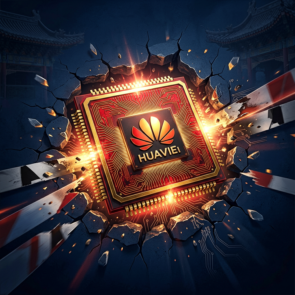
Huawei's announcement of a new chip design architecture — dubbed "Logic folding" or the "Tau scaling law" by industry observers — has sent shockwaves through the global semiconductor industry. The company claims this breakthrough will allow it to achieve transistor density equivalent to 1.4-nanometer processes by 2031, all without relying on the extreme ultraviolet (EUV) lithography machines that form the backbone of modern advanced chip manufacturing. If true, this isn't just a technical achievement. It's a geopolitical earthquake.
The DeepSeek Parallel
Analysts are already calling this a "DeepSeek moment" for hardware — a reference to the Chinese AI startup that shocked the world in early 2026 by building a large language model competitive with OpenAI's best, using older, less powerful Nvidia chips and innovative software techniques. DeepSeek proved that clever engineering could overcome hardware limitations. Now Huawei is attempting the same feat in silicon.
The comparison is apt. DeepSeek's breakthrough came from optimizing software to run efficiently on constrained hardware. Huawei's approach appears to be the inverse: redesigning the hardware itself to work around manufacturing constraints. By rethinking how transistors are arranged and interconnected — the "logic folding" technique — Huawei may have found a path to advanced computing power that doesn't require the bleeding-edge lithography that ASML's EUV machines provide.
How the Workaround Works
Traditional semiconductor manufacturing follows a straightforward (if incredibly difficult) path: shrink the transistors, pack more onto a chip, and connect them with ever-finer wiring. This requires increasingly sophisticated lithography equipment — specifically EUV machines that cost $200 million each and are effectively controlled by the US, Netherlands, and Japan through the trilateral export agreement.
Huawei's approach, as described in technical analyses, appears to involve a fundamentally different strategy. Rather than shrinking individual transistors to atomic scales, the company is exploring three-dimensional architectures and novel interconnect strategies that increase effective density without requiring the same lithographic precision. The "Tau scaling law" suggests a mathematical framework for optimizing chip layouts that trades traditional 2D scaling for more complex 3D arrangements.
The result: chips that perform like 1.4nm products but are manufactured using equipment that China can still legally acquire — older deep ultraviolet (DUV) lithography machines, possibly with multi-patterning techniques that TSMC and Samsung used years ago before EUV was commercially viable.
Why This Matters for US Sanctions
The entire US strategy for containing China's semiconductor ambitions rests on a single assumption: that without access to EUV lithography, China cannot manufacture chips competitive with the global state of the art. This assumption has driven billions in subsidies for US chipmakers, endless rounds of export controls, and intense diplomatic pressure on allies to join the blockade.
Huawei's breakthrough, if validated, blows a hole in that strategy. It suggests that the US has been playing a game of whack-a-mole against an opponent with far more engineering creativity than anticipated. Every time Washington closes one door — banning EUV sales, restricting access to advanced design software, cutting off high-bandwidth memory — China finds another path.
The implications extend far beyond Huawei. If this architectural approach works, it could be adopted by China's entire semiconductor ecosystem — from state-backed giants like SMIC to the swarm of startups that have emerged in response to US pressure. China has already demonstrated its ability to mobilize national resources behind strategic technologies. A proven workaround for the EUV bottleneck would trigger an avalanche of investment and talent migration.
The Market Reaction
Within China, the reaction has been electric. The hashtag "Huawei Semiconductor Field New Breakthrough" generated 40 million views on Chinese social media within days of the announcement. State media has amplified the story as evidence of Chinese technological resilience and a repudiation of Western "containment" strategies.
Global markets have been more cautious. Semiconductor stocks saw modest volatility, but investors are waiting for independent verification of Huawei's claims. The semiconductor industry has a long history of companies announcing breakthroughs that fail to materialize in commercial products. Huawei itself has made bold claims before that took years to validate — if they were validated at all.
But the market's caution may be missing the point. Even if Huawei's specific claims are overstated, the direction is clear. China is investing hundreds of billions in semiconductor R&D, and the law of large numbers suggests that breakthroughs will happen. The only question is when, not if.
What Happens Next
For the US, Huawei's breakthrough presents an uncomfortable choice. Washington can double down on sanctions — attempting to restrict DUV equipment, design software, or even basic semiconductor materials — but each escalation risks alienating allies who are already chafing under US extraterritorial pressure. The Netherlands, home to ASML, has repeatedly pushed back against US demands to tighten export controls. Japan and South Korea, both major semiconductor suppliers, have their own economic interests to protect.
Alternatively, the US could pivot to a strategy of overwhelming investment — outspending China in R&D, subsidizing domestic manufacturing, and building alliances around shared technology standards. The CHIPS Act was a start, but at $52 billion, it's a fraction of what China is spending. And Huawei's breakthrough suggests that money alone may not be enough if the engineering creativity gap persists.
For China, the challenge is execution. Announcing a breakthrough is easy; mass-producing competitive chips is extraordinarily hard. SMIC, China's most advanced foundry, has struggled for years to achieve yields comparable to TSMC even at mature nodes. If Huawei's architecture requires equally precise manufacturing, the theoretical advantage may not translate to commercial reality for years.
But if Huawei succeeds — if it can deliver 1.4nm-equivalent chips in volume by 2031 — the global semiconductor landscape will be fundamentally altered. TSMC's dominance, built on decades of process leadership, would face a credible challenger. The US blockade would be exposed as a temporary speed bump rather than a permanent barrier. And the world would have to recalculate the balance of technological power.
🔥 Hot Takes
1. The US semiconductor blockade is officially a failed strategy. It was always based on the arrogant assumption that China couldn't innovate its way around hardware limitations. DeepSeek proved that assumption wrong in software. Huawei is now proving it wrong in hardware. Washington has spent five years and hundreds of billions building a wall, and China just walked around it. The only question now is whether policymakers will admit failure or double down on a losing hand.
2. TSMC should be terrified. For decades, TSMC's moat was simple: no one else could match its process technology. If Huawei's workaround actually works, that moat shrinks dramatically. TSMC would still lead in yield, reliability, and ecosystem support — but "slightly better" isn't a defensible position when your competitor is backed by the entire Chinese state and doesn't care about profit margins. TSMC's $100 billion Arizona investment is starting to look like a very expensive hedge against a threat that just got real.
3. This is the beginning of a bifurcated semiconductor world, not the end. Even if Huawei succeeds, we're not returning to a single global supply chain. We're heading toward two parallel ecosystems: one US-aligned (TSMC, Samsung, Intel) and one China-aligned (Huawei, SMIC, and the swarm of state-backed startups). The winner won't be determined by who has the best lithography — it'll be determined by who builds the better software ecosystem, the stronger partnerships, and the more resilient supply chains. And on those metrics, the race is a lot closer than Washington wants to admit.
Bottom line: Huawei's chip breakthrough isn't just about transistors and lithography. It's about whether technological containment works in a world where engineering creativity can overcome material constraints. The US bet that it could. Huawei just called that bet — and the pot is the future of global technology leadership.